
Fujifilm invests in electronics
Submitted by:
Andrew Warmington
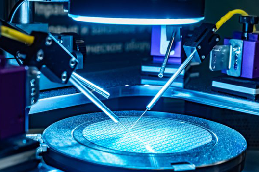
Fujiflm will spend about €25 million to install new facilities for chemical-mechanical planarisation (CMP) and advanced semiconductor materials, and to enhance existing facilities for photolithography-related materials, at Zwijndrecht, Antwerp. It had previously added development, production and quality evaluation functions for advanced resists at Shizuoka, Japan, and Pyeongtaek, Korea and expanded CMP slurry facilities at Kumamoto, Japan.
The company said that the investment will create a global production network of six locations, including others in Taiwan and the US. It should thus ensure a more stable supply of CMP slurries, demand for which is forecast to grow at about 13%/year. Globally, Fujifilm plans to invest nearly €1.1 billion over three years in both R&D and capital investment in semiconductor materials.