Fujifilm adds to semiconductor materials
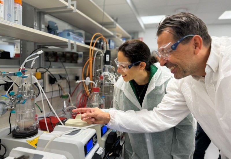
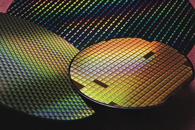
Japan’s Fujifilm Electronic Materials is to invest about $140 million to enhance the development, production and quality evaluation functions for advanced semiconductor materials at two sites in Japan. This comes in response to growing demand for semiconductors in both volume and quality terms and follows the start-up of a CMP slurries plant at Kumamoto in January.
At the Shizuoka site, the company will spend around about $91 million on a new building for advanced photoresists, including for extreme ultraviolet lithography (EUV), and for its Wave Control Mosaic products. Features will include a cleanroom and advanced inspection equipment. This scheduled to open in Q3 2025.
At Oita, meanwhile, Fujifilm will spend about $49 million on another new building on land adjacent to the existing site in 1H 2026. It will introduce additional production equipment and inspection devices to expand by 40% its capacity for post-CMP cleaners. These are used to remove particles, minute metal fragments and organic residues after polishing with CMP slurry.
RELATED ARTICLES